


ミッション
OIST のエンジニアリング部門は、実験装置、サンプル、デバイスの設計、製造、特性評価において研究者を支援することで研究を推進しています。
私たちの専門スタッフチームは、以下のようなサポートを提供しています:
- メカニカルエンジニアリング
- エレクトロニクス
- ナノファブリケーションとマイクロファブリケーション
- 光学特性評価
- 物理特性評価
- 材料と構造の特性評価
教育、ユーザートレーニング、沖縄の産業界や地域社会へのアウトリーチは、私たちの最優先事項のひとつです。


OIST のエンジニアリング部門は、実験装置、サンプル、デバイスの設計、製造、特性評価において研究者を支援することで研究を推進しています。
私たちの専門スタッフチームは、以下のようなサポートを提供しています:
教育、ユーザートレーニング、沖縄の産業界や地域社会へのアウトリーチは、私たちの最優先事項のひとつです。

工作室は、ラボ2の近くにある専用の施設(ESB)内に設置されています。訓練を受けた技術スタッフが、手動工作機械から全自動の多軸工作機械まで、多岐にわたる機器の利用をサポートしています。

当セクションのナノファブリケーション施設は、2つのクラス1000クリーンルームを中心に構成されており、マイクロおよびナノスケールのサンプル製造のための設備が整っています。最先端の成膜装置、(電子ビーム)リソグラフィー、3Dプリンティング、エッチングツール、集束イオンビームを駆使し、専門スタッフがあなたの目標達成のお手伝いをします。クリーンルームはラボ2と5にあります。

サンプルやデバイスの包括的な特性評価は、クリーンルーム内および周辺にある様々な装置で行うことができます。これには、ラボ4にある光学的、構造的、物理特性評価システムも含まれます。

当セクションのエレクトロニクスチームは、回路設計やエレクトロニクスのあらゆるニーズに対して専門的なサポートを提供します。プリント基板(PCB)の製造やデバイスのプロトタイプの組み立てから、信号解析、診断、コンサルティングに至るまで、課題の解決をサポートし、あなたのアイデアを実現へと導きます。

OISTのエンジニアリングセクションは、全キャンパスの施設や研究室において、レーザーシステムの設置や安全のコンプライアンス基準を満たすためのガイダンスを提供しています。
OISTの安全衛生規則に従い、OISTでは、レーザーを使用する方々やレーザー管理区域に立ち入る方々を対象に、実践的なレーザー安全教育を提供しています。OISTレーザー安全諮問委員会と協力し、OIST職員、学生、客員研究員を問わず、全てのレーザー利用者のためにレーザー安全の向上に努めています。
New equipment, events and publications by fiscal year (April to March), plus one combined list of publications.
Fiscal year 2026 is in progress. Entries are added as the year goes on.
Seven new tools added thin-film deposition, laser micromachining, thin-film metrology and three machine tools.
| Equipment | Inventory ID | Location |
|---|---|---|
| Kurt J. Lesker PRO Line PVD 75 sputter deposition system | ENG-N062 | L5-D46 |
| LightFab 3D Printer M (selective laser etching and direct laser writing) | ENG-N063 | L4-D36a |
| Sentech SER800 spectroscopic ellipsometer | ENG-N066 | L5-D49 |
| Bruker Dektak Pro A mechanical profiler | ENG-N069 | L5-D49 |
| Hurco VM20i 4th-axis vertical machining center | ENG-M046 | ES110 |
| Sharp 1118H high-precision collet lathe | ENG-M049 | ES110 |
| TRAK K3KMX-3 CNC knee-type milling machine | ENG-M048 | ES110 |
What it does: Box-style magnetron sputtering system with four 2-inch targets (Al, Ti, Cr, ITO, Si₃N₄, SiO₂ and Nb; others on request). DC and RF power, reactive sputtering for oxides and nitrides, substrate heating to 350 °C and rotation, base pressure around 8 × 10⁻⁸ torr, and substrates up to 6 inches through a load lock.
Typical applications: Metallization, transparent electrodes (ITO), optical and passivation coatings, and multilayer thin-film R&D.
Access: User / staff operated. Open to external use.
What it does: Industrial femtosecond/picosecond laser workstation (1030 nm, 8 W or more) for selective laser etching (SLE) of fused silica, Borofloat and sapphire, and for direct laser writing and ablation of graphite, ceramics, metals, plastics and optical-fiber facets. A 3-axis stage with 3 nm XY resolution supports wafer-level and curved 3D writing.
Typical applications: Microfluidics, integrated optics, MEMS, glass welding, fiber-facet processing, and rapid prototyping of 3D glass and multi-material parts.
Access: User / staff operated. Open to external use.
What it does: Non-destructive measurement of thin-film thickness (1 nm to 25 µm, accuracy around 1 nm) and optical constants (n, k) across 240–1050 nm. A spectrum takes about 300 ms, samples up to 6 inches, with recipe-based software and material libraries.
Typical applications: Characterizing semiconductor and dielectric films, optical coatings and photovoltaic materials, for example checking film thickness after sputtering, CVD or ALD.
Access: User / staff operated. Open to external use.
What it does: Stylus profiler for surface topography, roughness and step height, with 0.1 nm vertical resolution, scans up to 55 mm (stitchable to 200 mm) and a low-force sensor (0.03–15 mg) for delicate surfaces. Vision64 software provides 2D/3D analysis.
Typical applications: Thin-film and etch-depth metrology, lithography process control, surface roughness, and film stress or wafer bow.
Access: User / staff operated. Open to external use.
What it does: Vertical machining center with a 4th axis, 1,016 × 508 × 508 mm travels, a 12,000 rpm spindle and a 24-tool automatic changer, run by Mechanical Engineering staff.
Typical applications: Complex custom parts and prototypes in metals and plastics, including multi-face and rotary features that would otherwise need several setups.
Access: Staff operated. External use by consultation.
What it does: Toolroom lathe with spindle accuracy within 50 millionths of an inch TIR, variable speed from 50 to 4,000 rpm and 36 inch/metric thread changes. Built for small parts that need threading, with fast turnaround.
Typical applications: Small precision shafts, pins, fittings and threaded components for experimental setups.
Access: Staff operated. External use by consultation.
What it does: Three-axis CNC knee mill with a 10 × 50 in table, 32 in of table travel, a 3 HP spindle and a head that tilts 45° forward/back and 90° left/right.
Typical applications: Fast-turnaround brackets, fixtures, mounts and one-off parts for laboratory setups.
Access: Staff operated. External use by consultation.
Six new nanofabrication tools expanded lithography, deposition, etching and surface cleaning in Lab 5.
| Equipment | Inventory ID | Location |
|---|---|---|
| Elionix ELS-Boden 100 electron beam lithography system | ENG-N054 | L5-D48 |
| Heidelberg Instruments MLA 150 maskless aligner | ENG-N055 | L5-D48 |
| Samco AD-800LP plasma-enhanced atomic layer deposition (PE-ALD) system | ENG-N053 | L5-D46 |
| Samco RIE-200NL reactive ion etching system | ENG-N059 | L5-D46 |
| Samco PD-220NL plasma-enhanced chemical vapor deposition (PECVD) system | ENG-N057 | L5-D46 |
| Diener Electronic Atto plasma cleaner | ENG-N058 | L5-D48 |
What it does: Direct-write electron beam lithography for nanoscale patterning. A thermal field-emitter source at a fixed 100 kV gives a beam down to 1.8 nm, minimum line widths of 6 nm and ±10 nm field-stitching and overlay accuracy, on samples from 5 × 5 mm pieces to 6-inch wafers. Layouts are prepared in BEAMER/TRACER and accepted as GDSII or DXF.
Typical applications: Nanophotonics, quantum devices, nanoelectronics and advanced-materials research; any work that needs mask-free, high-fidelity patterning with precise alignment.
Access: User operated. Open to external use.
What it does: Maskless photolithography using 405 nm or 375 nm diode lasers and a digital micromirror array, so no photomask is needed. Minimum feature size is 600 nm, with front- and back-side alignment and write speeds up to 285 mm²/min on substrates from 5 × 5 mm to 6-inch wafers.
Typical applications: Rapid prototyping, MEMS, micro-optics and sensor fabrication, and small-batch multi-layer device patterning.
Access: User / staff operated. Open to external use.
What it does: Thermal and plasma-enhanced atomic layer deposition of oxides (Al₂O₃, SiO₂, TiO₂) and nitrides (AlN, Si₃N₄, TiN). An inductively coupled plasma source (up to 300 W) allows film growth at lower temperatures than thermal ALD, on samples from 5 × 5 mm to 6-inch wafers, loaded through a load lock.
Typical applications: Conformal, atomically controlled thin films on temperature-sensitive substrates, such as dielectric, barrier and passivation layers.
Access: User / staff operated. Open to external use.
What it does: Capacitively coupled reactive ion etching of silicon-based materials such as SiO₂ and SiN, other oxides and nitrides, and some metals. RF power up to 600 W, a chiller-controlled electrode and a built-in HORIBA laser-interferometric endpoint monitor that detects etch completion in real time. Samples from 5 × 5 mm to 4-inch wafers.
Typical applications: Pattern transfer after lithography, and etching of thin films and multilayer stacks with reliable endpoint control.
Access: User / staff operated. Open to external use.
What it does: Plasma-enhanced chemical vapor deposition of silicon dioxide, silicon nitride and amorphous silicon. Capacitively coupled RF plasma (up to 300 W), substrate temperatures up to 400 °C, deposition rates above 100 nm/min and up to 4 µm per run, on samples up to 4-inch wafers.
Typical applications: Dielectric and passivation layers, hard masks, and films for microelectronics and photonics devices.
Access: User / staff operated. Open to external use.
What it does: Low-pressure RF plasma cleaner (10–300 W, oxygen and/or argon) that removes organic contamination, activates surfaces to improve adhesion, and modifies surface wettability and chemistry.
Typical applications: Cleaning and activating samples before lithography, deposition, bonding or coating.
Access: User / staff operated. Open to external use.
Vacuum Day, January 22, 2025. The Engineering Section, Pfeiffer Vacuum, Hakuto Co. and Tomy hosted a full-day program at OIST with lectures on the basics of vacuum technology, hands-on training and presentations of new vacuum solutions. 40 participants attended.
Publications connected to the Engineering Section, newest first.
Depending on the nature of your request, please click on the sections relevant to your needs...
The Mechanical Team offers design consultation, custom machining, welding, forming and 3D Printing to meet the needs of researchers here at OIST.
To request the fabrication/modification of your parts please use the following links:
To request a consulation or to submit a job please use this link: JOB SUBMISSION.
Please include:
When a complex mechanical problem presents itself and requires a solution, please reach out to the Mechanical Team for help. Our specialists will use their many years of experience to help you get the desired result.
Our specialists can also assist in the the designing of parts and assemblies for fabrication.
For consultation & advice please click here: DESIGN CONSULTATION and let us know the details of your project. If the problem is urgent please stop by our office located in the Engineering Support Building (ES-102).
For training please submit a request through PPMS here: TRAINING REQUESTS and let us know your needs. A brief consulation about your needs may be required before training is approved, and a date for training given.
The training is given by one of our specialists who will guide you through the safe operation of the equipment. Training is held on a the following schedule each month:
All training sessions are limited to 5 trainees.
The OIST machine shop (Engineering Support Building) is the main area for the fabrication and assembly of custom parts in the university, with a range of state of the art staff operated machine tools present. It is also home to the users corner, where user-operated machine tools are located.
All OIST researchers are welcome to use the users corner facilities after carrying out induction, which includes the following steps:
1. Online learning
The first step to gaining access to the machine shop users corner is to complete online training available on OIST Learn (E-Front Pro).
2. Staff Induction (Basic training)
The second step is to attend a comprehensive induction to the machine shop conducted by one of our specialists. This deals with all the practicalities of the machine shop:
The induction by staff is held on the first FRIDAY of each month. The number of spaces is limited to 3 per session, registration is necessary by e-mailing mechanical@oist.jp.
Note: Completing the induction will not grant key card access to the machine shop which is limited for safety reasons.
Visiting researchers and collaborators should follow the same procedure as above, after the hosting research unit has completed the relevant steps as laid out here.
Safety
The safety of everyone working at OIST is always the top priority of the section. Within the section we strive to provide the safest working environment for all users.
To do this we require all users to be aware of safety protocols here at OIST and to work in the safest possible manner. Before beginning work please:
The machine shop is located in the Engineering Support Building, 1F, Room ES110:
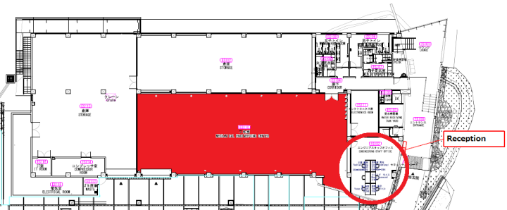
Training by a member of staff is available upon request for the nanofabrication and characterization equipment managed by the section. The training is given by one of our specialists who will guide you through the operation of the equipment.
For general training inquiries please use our consultation request form. For specific training requests visit our PPMS page.
You will also need to request access to the cleanroom facilities (see section "Cleanrooms" below).
When fabrication or measurement aren't going as expected, or you are unsure which equipment or technique will give you the best results. One of our specialists may be able to help you get the desired result.
For consultation & advice please fill our consultation form and let us know the details of your project.
When fabricating or measuring samples, the helping hand of an experienced user is often useful. In this case our specialists can work with you to develop a fabrication process, or in taking a measurement.
To request our assistance please fill our consultation form and let us know the details of your project.
On some occasions a researcher may request for the item to be fabricated or measured by the section staff.
As this is the most time consuming service the section staff can offer it is only available in some cases, dependent on the project and availability of staff.
To request staff operation please fill our consultation form and let us know the details of your project.
It is important to remember when requesting the services above that staff time is limited. With increasing involvement in projects, the fewer projects can be taken on by staff members who have a range of duties to attend to.
Safety
The safety of everyone working at OIST is always the top priority of the section. Within the section we strive to provide the safest working environment for all users.
To do this we require all users to be aware of safety protocols here at OIST and to work in the safest possible manner. Before beginning work please:
Our micro/nanofabrication facilities are centered around our two Class 1000 cleanrooms, which are equipped for fabrication of samples on the nanoscale. Using the state of the art deposition, lithography and etching tools our expert staff can help you to achieve your goals. Cleanrooms are located in Labs 2 and 5.
All OIST researchers are welcome to use the facility after carrying out induction, which includes the following steps:
1. Online Learning
The first step to gaining access to the cleanroom is to complete online training available on OIST Learn (eFront Pro).
2. Cleanroom Induction (Walk around)
The second step is to attend induction given by a staff member, detailing the practical side of the cleanroom:
The induction by staff is held only on request, meeting outside of the cleanroom. Contact nanofab@oist.jp to put in your request.
3. Room access request webform
The final step is to submit a room access request via Building Facilities Management
Visiting researchers and collaborators should follow the same procedure as above, after the hosting research unit has completed the relevant steps as laid out here.
The cleanroom is located in Lab 2, Level A, Room A645 and Lab 5 D-level.
Training by a staff member is available upon request for the electronics equipment managed by the section. The training is given by one of our specialists who will guide you through the equipment's operation.
For training, please contact electronics@oist.jp and let us know the following information:
When the design, fabrication, assembly, or measurement aren't going as expected for your circuit. Or you are unsure about the equipment, component, or technique that will give you the intended results.
For consultation & advice, please contact electronics@oist.jp and let us know the details of your project.
When fabricating or measuring samples, the helping hand of an experienced user is often useful. In this case, our specialists can work with you to develop a design, assemble a circuit, or take measurements.
To request our assistance, please contact electronics@oist.jp and let us know the details of your project.
On some occasions, a researcher may request for the item to be designed, fabricated, or measured by the section staff.
As this is the most time-consuming service the section staff can offer, it is only available in some cases, depending on the project and staff availability.
To request staff operation, please contact electronics@oist.jp and let us know the details of your project.
It is important to remember when requesting the services above that staff time is limited. With increasing involvement in projects, fewer projects can be taken on by staff members who have a range of duties to attend to.


