


16 June 2026
New high-NA lithography optical system design aims to revolutionize semiconductor chipmaking

From data centers powering next-generation AI, to vital medical technology, to cars, and to the very mobile device or computer that you’re probably reading this on, semiconductor-based computer chips are essential for modern life.
As technology advances and power consumption increases, scientists are hoping to create ever smaller computer chips, requiring delicate chip designs on the individual nanometer (nm) scale. Methods such as extreme ultra-violet (EUV) lithography are providing new paths to these smaller chips, but come with major physics, engineering and financial challenges, limiting current application and scalability.
Published on June 12 in the Journal of Micro/Nanopatterning, Materials, and Metrology (JM3), Professor Tsumoru Shintake of the Okinawa Institute of Science and Technology (OIST), has proposed a radical redesign to the illumination systems and projectors used in high numerical aperture (high-NA) EUV lithography. Simulations suggest that his design could eliminate troublesome optical (so-called ‘mask 3D’) effects, enhance resolution and enable the manufacture of smaller computer chips at lower cost than current EUV methods.
Shintake says, “Current EUV lithography systems cost hundreds of millions of euros per machine. My new design should achieve fine, 2-3 nm scale details, in a much cheaper way compared to today’s state-of-the-art machines.”
He highlights the downstream applications of these smaller semiconductor chips in the context of growing AI demands.
“The International Energy Agency predicts that data center electricity consumption will double by 2030, due to demand from energy-intensive applications like AI agents. However, the higher density of features on high-NA-produced chips means signals should travel shorter distances, minimizing energy loss. This can reduce power cost per computation,” explains Shintake. “These denser chips should also release less heat, lowering power required for cooling. Such improvements could have significant impacts for data center energy usage.”
What is EUV lithography? Understanding semiconducting chip synthesis
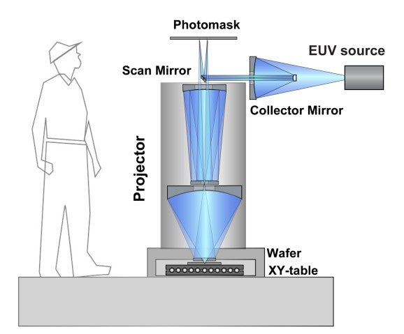
In EUV lithography, light with an extremely short wavelength (13.5 nm) is generated and guided through an illumination system, where it strikes a reflective photomask that contains a template of the circuit pattern. The reflected light pattern then passes through a projector, which uses a series of mirrors to shrink and focus the image onto a silicon wafer. The pattern is then etched onto the wafer through further processing.
To print a higher density of circuit components, researchers are turning to high-NA EUV lithography. NA is linked to the range of angles at which an optical system can accept or emit light. A higher NA captures a wider angle of light, enabling the lens to resolve finer details. In theory, the resolution limit (the smallest detail that can be resolved) is inversely proportional to NA, so a higher NA provides the finer printing capability for semiconductor chips.
In the early days of EUV lithography research in the 1990s, scientists had explored optical designs for high-NA lithography that were similar to Shintake’s, in which the photomask, projector, and wafer were aligned. While these in-line configurations were attractively simple, researchers were unable to find solutions to distortions, blurring, and other optical errors that occurred, particularly as the NA increased.
To address these challenges, Shintake first investigated whether a simple pair of mirrors — one concave and one convex — could serve as the projector. His design eventually evolved into a two-stage configuration, with a concave-convex mirror pair in each stage. While initially unsuccessful, Shintake soon realized that multiple reflections between carefully arranged mirrors could potentially cancel out optical defects while maintaining high NA. After spending many months running calculations on OpTaliX, an optical simulation system, he determined the ideal curvature and positioning of the mirrors needed to achieve high NA while preserving image quality.

A step towards scalable semiconductor production
As with every research project, there are some limitations. The simulations assume that mirrors will be 100% reflective and defect-free, and moving from simulation to real-world implementation will require expert engineering. Building a physical prototype is Shintake’s next step, and his team has now started developing EUV hardware, with the aims of producing lower cost, high performance EUV lithography.
“This design can make high-NA technology much simpler and cheaper to produce, opening new possibilities for semiconductor manufacturing. We should be able to create machines that are a quarter of the cost of those currently on the market,” concludes Shintake. “By achieving finer designs, we can make higher density memory and more efficient logic chips. This technology may have transformative impacts on society, powering data centers and the future of AI, and making electronics faster, more energy efficient and potentially cheaper to run.”
Article Information
Specialties
Research Unit
Submit a press inquiry


