17 September 2015
Laser Ablation Boosts Terahertz Emission
From almost instantaneous wireless transfer of huge amounts of data and easy detection of explosives, weapons, or harmful gases, to safe 3-D medical imaging and new advances in spectroscopy — technologies based on terahertz (THz) radiation, the electro-magnetic band with wavelengths from 0.1 to 1 mm, can transform science fiction into reality. However, scientists and engineers still do not have cheap and efficient solutions for mass production of THz-based devices.
For years, the THz portion of the spectrum remained unused giving rise to the term “terahertz gap”. Research, recently published in Optics Letters by the Femtosecond Spectroscopy Unit, led by Prof. Keshav M. Dani, at the Okinawa Institute of Science and Technology Graduate University (OIST), suggests one possible solution for this problem: a method to increase efficiency of THz emission gallium arsenide (GaAs)-based devices.
THz radiation lies between infrared and microwave radiation in the electro-magnetic spectrum. It is absorbed by water — which limits the use of THz devices in the Earth's atmosphere, laden with water vapour, to short distances — but it can penetrate fabrics, paper, cardboard, plastics, wood, and ceramics. Many materials have a unique “fingerprint” in the THz band allowing their easy identification with THz scanners. Moreover, unlike X-rays and ultraviolet light, THz radiation is safe for live tissues and DNA due to its non-ionising properties. THz technology could be a next important breakthrough in medicine, security, chemistry, and information technology.
Generation of THz waves is difficult since the frequency is too high for conventional radio transmitters, but too low for optical transmitters, like the majority of lasers. Therefore, researchers have to come up with new innovative devices.
One of the most frequently used THz emitters is a photoconductive antenna, comprising two electric contacts and a thin film of semiconductor, often GaAs, between them. When the antenna is exposed to a short pulse from a laser, the photons excite electrons in the semiconductor and a short burst of THz radiation is produced. Thus the energy of the laser beam is transformed into a THz electro-magnetic wave.
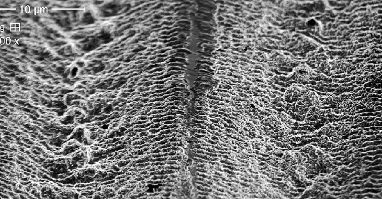
OIST researchers showed that micro-structure of the semiconductor surface plays an important role in this process. Femtosecond-laser-ablation, in which the material is exposed to ultrashort bursts of high energy, creates micrometre-scale grooves and ripples on the surface of GaAs. “The light gets trapped in these ripples”, says Athanasios Margiolakis, a Special Research Student at OIST. Since more light is absorbed by the ablated material, the efficiency of THz emission, given a sufficiently powerful laser, increases by 65%.
Other properties of the material change as well. For example, ablated GaAs shows only a third of the electrical current of non-ablated GaAs. “We observe counter-intuitive phenomena,” the researchers write, "One generally expects that the material showing the higher photocurrent would give the best THz emitter.” They explain this phenomenon by shorter carrier lifetimes. That is, electrons in ablated samples return to non-agitated states much faster than in control samples.
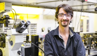
Dr Julien Madéo, one of the OIST team members, says that “femtosecond-laser ablation allows us to engineer the properties of materials and to overcome their intrinsic limitations, leading, for example, to near 100% photon absorption as well as broader absorption bandwidth, control of the electron concentration and lifetime”. This technique is a fast, lower-cost alternative to existing methods of manufacturing materials for THz applications.
Specialties
Research Unit
Submit a press inquiry


