


09 March 2022
Scientists capture the fleeting dance of moiré excitons

Highlights
- Scientists have utilized a powerful and precise technique to image a unique particle, called a moiré exciton.
- Excitons are hailed as having the potential to revolutionize technological and quantum devices, but they’re usually fleeting in nature, which makes them difficult to study.
- Moiré excitons have longer lifespans as they are formed between two semiconducting layers, which have been stacked together and aligned to create a moiré pattern—a landscape of electronic energy.
- For the first time ever, scientists were able to visualize the hole of the exciton, paving the way for more complex research.
- Using the images of both the electrons and the holes of moiré excitons, the researchers found that the excitons were very localized by the moiré pattern and formed in places where the energy was minimal.
Press release
Published in leading journal Nature, scientists from the Okinawa Institute of Science and Technology Graduate University (OIST), SLAC National Accelerator Laboratory (SLAC), and Stanford University have, in a world-first, imaged and measured the two parts of a unique particle, called a moiré exciton. Excitons are hailed as having the potential to revolutionize technological and quantum devices, but they are usually fleeting in nature, often lasting no longer than a few thousandths of a billionth of a second, which makes them incredibly difficult to study. Moiré excitons tend to be longer-lived and are thus an attractive way to study the particle and its potential applications. Yet information about their size, shape, and behavior remains unclear.
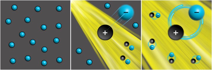
Excitons are created when light is shone on a semiconducting material. The particles of light, called photons, interact with the material’s electrons. This causes the electrons to jump to a higher energy level. Each one leaves behind a hole at the lower energy level. The two are oppositely charged so they mutually attract and revolve around each other, forming the short-lived exciton.
“We’ve previously visualized the electron part of the exciton before it disappeared,” stated Mr. Vivek Pareek, one of the six first authors in this paper and PhD candidate in OIST’s Femtosecond Spectroscopy Unit. “In this new study, we measured both parts of the exciton. This was the first time we’ve seen the ‘hole’, or lack of an electron.”
“This is really exciting research and could have vast implications,” added Dr. Michael Man, a staff scientist in the same unit and also one of the first authors. “Excitons adopt the properties of the material they’re in. By controlling the materials and the environment of the excitons, we can control the exciton itself.”
In the previous research, the scientists visualized excitons in a two-dimensional, single layer semiconductor. Now, the researchers have stacked two semiconducting layers on top of each other. When the exciton forms, the electron jumps from one layer to the other. This forces the electron and hole to remain apart for longer, extending the lifespan of the exciton.
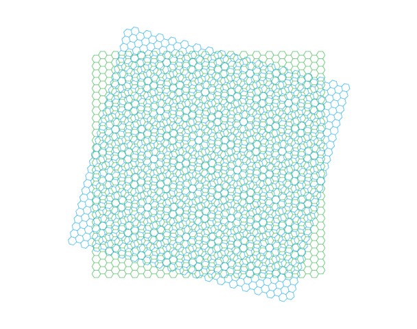
The two-dimensional, two-layered samples were created in the state-of-the-art laboratories at SLAC and Stanford University. The two layers had to be aligned in a very specific way to create a pattern, called a moiré pattern.
“Imagine that the atomic structure of the two different materials are like two nets. The structures resemble each other but they are not exactly the same,” explained Dr. Ouri Karni, also a first author and a postdoctoral researcher working in the group of Prof. Tony Heinz at SLAC and Stanford University. “When the nets are placed on top of each other, there are certain places where the gaps in the nets overlap, and others where they do not. This results in a moiré pattern. We aligned these atomic ‘nets’ at very specific angles so they would clearly exhibit the moiré pattern, which in turn expresses what is called moiré potential—a periodic ‘landscape’ of electronic energy levels across the material.”
The samples were then sent to OIST where scientists utilized a powerful and unique technique. They shone a beam of light within the extreme ultraviolet range at the material. The energy was so high that the excitons were broken apart and their electrons were sent flying out of the material. By measuring the speed and angles of the electrons as they left the material, the scientists were able to backtrack this information and construct an image of the exciton.
Perhaps the most important and exciting part of this research, both conceptually and experimentally, was that the scientists were also able to see the hole. Since the hole is actually the absence of an electron, it doesn’t emit any of its own signals and its presence can only be detected by what is around it, similar to how black holes are detected.
“This is an incredibly powerful tool, which allowed us to obtain a full picture of the exciton–how far apart the electron and hole were from each other, and how much the two moved together in the material,” said Mr. Jonathan Georgaras, another first author and PhD candidate in Prof. Felipe Jornada’s theory group at Stanford University.
Furthermore, they were also able to estimate how many excitons were present, something they were unable to do with just the electron signals.
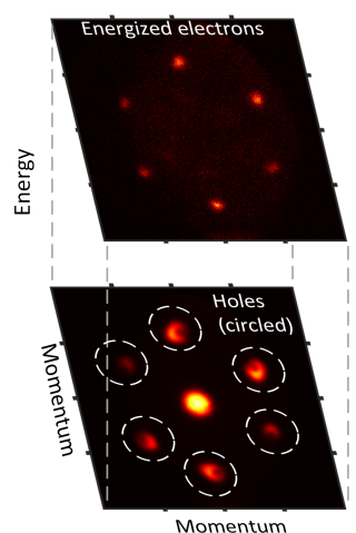
The researchers found that, due to the moiré potential, the excitons were very localized and formed in places where the energy was minimal. This meant that the excitons were effectively pinned in tiny pockets of around 1.8 nanometers, despite their relatively large diameter, at around 5.2 nanometers.
“After nearly a century of knowing about the existence of excitons, we are now able to get a near-holistic view of this important particle by peering into it and imaging both its constituent particles,” concluded Prof. Keshav Dani, who leads OIST’s Femtosecond Spectroscopy Unit and is a senior author of the paper. “This research opens the doors to studying more sophisticated phenomena with excitons for quantum technology. Our current demonstration of the pinning of the large moiré exciton in tiny pockets is just the beginning.”
Research information
- Title: Structure of the moiré exciton captured by imaging its electron and hole
- Journal: Nature
- DOI: 10.1038/s41586-021-04360-y
- Authors: Ouri Karni, Elyse Barré, Vivek Pareek, Johnathan D. Georgaras, Michael K. L. Man, Chakradhar Sahoo, David R. Bacon, Xing Zhu, Henrique B. Ribeiro, Aidan L. O’Beirne, Jenny Hu, Abdullah Al-Mahboob, Mohamed M. M. Abdelrasoul, Nicholas S. Chan, Arka Karmakar, Andrew J. Winchester, Bumho Kim, Kenji Watanabe, Takashi Taniguchi, Katayun Barmak, Julien Madéo, Felipe H. da Jornada, Tony F. Heinz, and Keshav M. Dani
- Affiliations: SLAC National Accelerator Laboratory; Stanford University; Okinawa Institute of Science and Technology Graduate University; Columbia University; National Institute for Materials Science
Specialties
Research Unit
Submit a press inquiry


