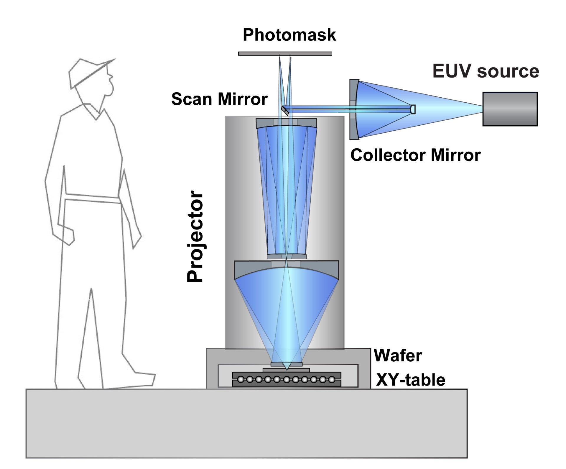



Simplified projector design

This diagram shows Shintake’s proposed high-NA EUV lithography projector design. The collector mirrors in the illumination system have a simpler design to bring short wavelengths of light from the EUV source to the photomask. The two sets of mirrors in the projector increase numerical aperture. The circuit pattern on the photomask is projected onto the wafer, followed by chemical etching that produces dense nanometer lines on the silicon surface. This process is carried out on more than 20 layers of wafer that are stacked to ultimately produce a functional chip.
Date:
16 June 2026
Credit:
Tsumoru Shintake, OIST
Copyright OIST (Okinawa Institute of Science and Technology Graduate University, 沖縄科学技術大学院大学). Creative Commons Attribution 4.0 International License (CC BY 4.0).
Share on: