


Researchers from the Femtosecond Spectroscopy Unit at OIST are investigating the fundamental properties of semiconducting materials that are promising candidates for next-generation solar cells.
They use cutting-edge materials characterization techniques to study electron dynamics in novel materials, focusing on detrimental processes which can impact the performance and stability of energy devices. By combining high-temporal resolution techniques (i.e., femtosecond pump–probe spectroscopy) with an advanced imaging technique that provides high spatial resolution (i.e., photoemission electron microscopy), the researchers can study how electrons move in solar cell materials at fundamental timescales. This technique, called “time-resolved photoemission electron microscopy” is at the forefront of advanced materials characterization techniques, and few groups in the world have such capabilities available.
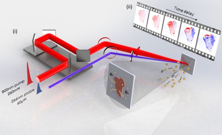
Previously, the unit has conducted research on imaging the ultrafast transfer of electrons through a prototypical material stack called a “type-II heterojunction”, which is the foundation for a solar cell device. Currently, they are focusing their efforts on investigating the source of efficiency-limiting defects in state-of-the-art hybrid organic-inorganic perovskites, materials that are expected to become future market leaders in the solar cell industry.
In the future, the unit plans to expand its research interests to study electron dynamics in semiconducting organic polymer blends. These materials form the basis of flexible organic solar cells, which are another promising alternative for future solar energy devices.
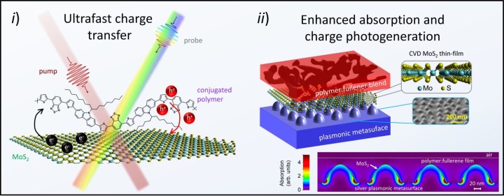
In addition to time-resolved photoemission electron microscopy, in the past the researchers have also utilized conventional ultrafast spectroscopy to study hybrid organic-2D heterojunctions, which are novel type-II heterojunctions between atomically-thin semiconductors and semiconducting organic polymer thin-films. This work has promising applications for the development of ultrathin optoelectronic devices.
The Femtosecond Spectroscopy Unit’s fundamental approach contributes to the development of renewable energy and is helping to guide future research towards the production of affordable and efficient solar cell materials.
Project Collaborators
- Stranks S. D., University Lecturer in Energy and Royal Society University Research Fellow, Optoelectronics Group, Cavendish Laboratory, University of Cambridge
- Manish Chhowalla, Goldsmiths’ Professor of Materials Science, University of Cambridge
Project Publications
- Man, M., Margiolakis, A., Deckoff-Jones, S. et al. Imaging the motion of electrons across semiconductor heterojunctions. Nature Nanotech 12, 36–40 (2017). https://doi.org/10.1038/nnano.2016.183
- Doherty, T.A.S., Winchester, A.J., Macpherson, S. et al. Performance-limiting nanoscale trap clusters at grain junctions in halide perovskites. Nature 580, 360–366 (2020). https://doi.org/10.1038/s41586-020-2184-1
- Petoukhoff et al. Charge transfer dynamics in conjugated polymer/MoS2 organic/2D heterojunctions. Molecular Systems Design & Engineering 4, 929-938 (2019). https://doi.org/10.1039/C9ME00019D
- Petoukhoff et al. Ultrafast Charge Transfer and Enhanced Absorption in MoS2–Organic van der Waals Heterojunctions Using Plasmonic Metasurfaces. ACS Nano 10, 11, 9899–9908 (2016). https://doi.org/10.1021/ACSNANO.6B03414


