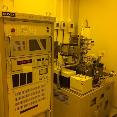
Electron Beam Lithography

The electron beam lithography (EBL) system is a nanofabrication tool used to write patterns onto a substrate coated with a sensitive resist with a focused electron beam. EBL systems offer high resolution, precise control over feature sizes, and flexibility in pattern design, making them essential to produce advanced electronic devices, photonic components, and nanostructures for various applications in science and technology.

Elionix Electron Beam Lithography

Basically, EBL generates and focuses electron onto the surface of a pre-coated substrate with an electro-sensitive resist. The control of the deflection, combined with the ability to blank the beam, allows the system to precisely pattern the substrate accordingly to the desired design. It has a conversion capability for previously generated CAD files. The Laser interferometer stage and 18-bit DAC beam positioning system provide excellent stitching and writing capabilities. The ELS-7500EX has a Zr/W thermal field emission electron gun source which offers a minimum beam diameter of 2nm at 50Kev accelerating voltage. It can produce ultra fine features down to a 10nm linewidth. The various stage options allow for patterning of substrate sizes ranging from small pieces (5x5mm) up to wafers that are 4" in diameter.

Share on:

Features

ZrO/W thermal field emitter Fixed acceleration voltage: 50 kV (lower voltage available 20 or 30kV)

Beam current: 10pa - 2nA 2nm minimum diameter spot Min. linewidth: 10nm (75µm field at 50kV) Stitching and overlay accuracy: <50nm Write field available: 75µm, 150µm, 300µm and 600µm Stage mouvement range : X: 100mm Y: 110mm Z: 5mm Sample size: from 5x5mm to 4-inch wafer Files supported GDSII or DXF (with data conversion)

Electron beam resists available: - PMMA 950k A4 - MMA - CSAR 62 (AR-P 6200) - AR-N 7511

More resists available on request.