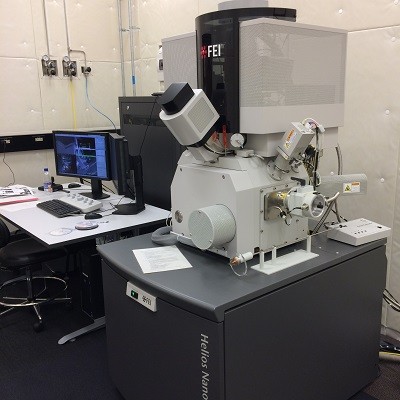
FIB-SEM Dual Beam
Features
Secondary electron (SE) imaging Backscattered electron (BSE) imaging Gas Injection System – platinum and carbon deposition Ion optics: Range acceleration voltage Ga ion: 500V to 30 kV Probe current: 0.1pA to 65nA 4.0nm resolution at 30kV Electron optics: Range SEM acceleration voltage: 350V to 5 kV Probe current: 0.8pA to 100nA 1.4nm resolution at 1kVPatterning: Maximum resolution: 64k x 64k Maximum pattern size: 16 mil. pixels per single pattern Minimum Dwell Time: 25 ns/pixel Maximum Dwell Time: 25 ms/pixel Complex milling patterns through Bitmap import GDSII file format support Feature sizes down to 20-30 nm (sample dependent) Maximum sample size: 110mm diameter Maximum sample thickness: 61mm incl. sample holder Stage tilt range -15 to +90°


